
|
| |
|
Строительный блокнот Introduction to electronics Converter Transfer Functions The engineering design process is comprised of several major steps: 1. Specifications and other design goals are clefined. 2. A circuit is proposed. This is a creative process (hat draws on the physical insight and experience of the engineer. 3. The circuit is modeled. The converter power stage is modeled as described in Chapter 7. Components and other portions of the system are modeled as appropriate, often with vendor-supplied data. 4. Desigii-orienred ajiaiy.vis of the circuit is performed. This involves development of equations that allow element values lo be chtjsen such that specifications and design goals are met. In addition, il may be necessary for the engineer to gain additional understanding and physical insight into the circuit behavior, so that the design can be improved by adding elements lo the circuit or by changing circuit connections. 5. Model verificariou. Predictions of the т(к1е1 are companjd to a laboratory prototype, under nominal operating conditions. The model is refined as necessary, so that the model predictions agree with laboratory measurements. 6. Worst-case analysis ior other reliability and production yield analysts) ofthe circuit is performed. This involves quantitative evaluation ofthe model performance, to judge whether specifications are met under all conditions. Compulersimulation is well-suited to this task. 7. Iteration. The above steps are repeated to improve the design until the worst-case behavior meets specifications, or until the reliability and production yield are acceptably high. This chapter covers techniques of design-oriented analysis, measurement of experimental transfer functions, and computer simulation, as needed in .steps 4, 5, and 6. Sections S.l to S.3 discuss techniques for analysis and construction of the Bode plots of the converter tran.sfer functions, input impedance, and output impedance predicted by the equivalent circuit Uiie input 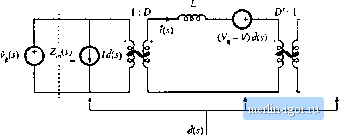 ОмрШ
Contrt input Ьщ, S.l Small-signal equivalent circuit niddel of the buck-boost ciniverter, И-ч derived in Chapter 7. models of Chapter 7, For example, the small-.signal equivalent circuit mt;idel of the buck-boo.sl convetter is illustrated in Fig. 7.17(c). This model is reproduced in Fig, 8.1, with the important inputs and terminal impedances identified. The line-to-output transferfnnction С ,(.у) is found by setting duty cycle variations to zero, aud then solving for the transfer function from iX-) to НУ- (8.1) This transfer function describes how variations or disturbances in the applied input vtdtage v{t) lead to disturbances in the output voltage vit). It is important in design of an output vtdtage regulator. Ftff example, in an off-line power supply, the converter input voltage v(l) contains nndestred even harmonics of the ac power line voltage. The transfer function O.i-i) is used t[;i detertnine the effect of these hartnonics on the converter output voltage v{t). The control-to-output transferfunction CrJs) is found by setting the input voltage variations v(.)>) to zero, and then solving the equivalent circuit model for v(s) as a function of rf(.v): il(s) (8.2) This transfer function describes how control input viuiations (lis) influence the output voltage In an output voltage regulattir system, (? ,/(.v) a key component of the loop gain and has a stgnificatit effect on regulator peifortnance. The output impedance 2 (*) is found under the conditions that i\.(i) and i/(.f) variations are set to zero. Z , (i) describes how variations in the load current affect the output voltage. This quantity is also important in voltage regulator design. It may be appropriate to define Z (j) either including or Qtit including the load resistance R. The conveiter input impedatice Z;;GO plays a significant mle when an electromagnetic interference (EMI) filter is added at the cotiverter power input. The relative tnagnitudes of Z, and the EMI filter output impedance influence whether the EMI filter disrupts the transferfunction (j\,Ji). Design of input EMI filters is the subject of Chapter 10. An objective of this chapter is the construction of Bode plots of the important transfer functions and terminal impedatices of switching converters. For example. Fig. 8.2 illustrates the magnitude atid phase plots of iov the buck-boust converter tnodel of Fig. 8.1. Rules for constructitm of magnitude and phase asymptotes are reviewed in Section 8.1, including two types of features that often appear in IIGII 80dBV 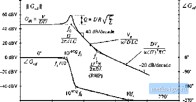 10 Hi 100 Hi IkHi lOkHi 100 kHz IMHi Fig. 8.2 Bode plot of control-to-Qutpiit triinsfer function predicted by the mode! of Fig. Я.1, with analytical expressions for the important features. converter transfer functions: resonances and right half-plane zeroes. Bode diagrams of the small-signal transfer functions ofthe btick-boost converter are derived in detail in Section 8.2, and the transfer functions ofthe basic buck, boost, and buck-boost converters are tabulated. The physical origins ofthe right half-plane zero are also described. A difficulty usually encountered in circuit analysis (step 5 ofthe above list) is the complexity of the circuit model: practical circuits may contains hundreds of elements, and hence their analysis may leads to complicated derivations, intractable equations, and lots of algebra mistakes. Dexign-oriemed a!Kdy.six[\] is a collection of tools and techniques that can alleviate these problems. Some tools for approaching the design of a complicated converter system are described in this chapter. Writing the transfer functions in normalized form directly exposes the important features of the response. Analytical expressions for these features, as well as for the asymptotes, lead to simple eqtiations that are useful in design. We 11-separated roots of transfer function polynomials can be approximated in a simple way. Section 8.3 describes a graphical method for constructing Btxle plots of transfer ftinctions and impedances, essentially by inspection. This method can: (1) reduce the amount of algebra and associated algebra mistakes; (2) lead to greater insight into circuit behavior, which can be applied to design the circuit; and (3) lead to the insight necessary to make suitable approximations that render the equations tractable. Experimental measurement of transferfunctions and impedances (needed in step 4, model verification) is disctissed in Section 8.5. Use of computer siinulation to plot converter transferfunctions (as needed in step 6, worst-case analysis) is covered in Appendix B. REVIEW OF BODE PLOTS A Bode plot is a plot ofthe magnitude and phase of a transfer function or other complex-valued quantity, vs. frequency. IVIagnitude in decibels, and phase in degrees, are plotted vs. frequency, using semiiogartth-mic axes. The magnitude plot is effectively a log-log plot, since the magnitude is expressed in decibels and the frequency axis is logarithmic. The magnittide of a dimensionless quantity G can be expressed in decibels as follows: |