
|
| |
|
Строительный блокнот Introduction to electronics region. This currem leads to a voltage drop in the resistance of Ihsp material, which influences the voltage across the base-emitterjimction. During the turn-off transition, the base current -/j causes the base-emitter junction voltage to be greater in the center of the base region, and smaller at the edges near the base contflcts. This causes the collector current to focus near the center of the base region. In a similar fashion, a large /д, causes the collector current to crowd near the edges of the base region during the turn-on transition. Since the collector-to-emitter voltage and collector current are simultaneously large during the switching transitions, substantial power loss can be associated with current focusing. Hence hot spots are induced at the center or edge of the base region. The positive temperature coefficient of the base-emitter junction current (corresponding to a negative temperature coefficient of the junction voltage) can then lead to thermal runaway and device failure. Thus, to obtain reliable operation, it may be necessary to limit the magnitudes of/ and It may also be necessary to add external siiu!)ber networks which the reduce the instantaneous transistor power dissipation during the switching transitions. Steady-state characteristics of the BJT are illustrated in Fig. 4.35. In Fig. 4.35(a), the collector current /is plotted as a function of the base current /д, for various values of collector-to-emitter voltage V(-.jr.The cutoff, active, quasi-saturation, and saturation regions are identified. At a given collector cur- 200 V 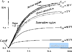 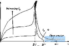 CEO CBO CB Fig. 4.35 BJT static characteristics: (a) vs. /д, illustrating tlio regions of operaliott; (b) vs. . illustrating voltage breakdown characteristics. rent If.., to Operate in the saturation region with rrtininiuni forward voltage drop, the base current !/) must be sufficiently large. Tire slope dlJdl/ in the active region is tire current gain P. it can be seen that fl decreases at high current-near the rated current of the BJT, tiie current gain decreases rapidly and hence it is difTtcult to fully saturate the device. Collector cuirent l(~ is plotted as a function of collector-to-emitter voltage Vf.f in Fig. 4.35(b), for various values of/д. The breakdown voltages BV BVfu. anJ aio illustrated. BVq is the avalanche breakdown voltage of the base-collector junction, with the emitter open-circuited or with sufficiently negative basecurrent. BV is the .somewhat smaller coUec-tcn-emitter breakdown voltage cjbserved when the base current is zertj; as avalanche breakdown is approached, free carriers are created that have the same effect as a positive base current and that cause the breakdown voltage to be reduced. BVjj, is the breakdown voltage observed with positive base current. Because of the high instantaneous power dissipation, breakdown usually results in destruction of the BJT. In most applications, the off state transistor voltage must not exceed BV-,. High-voltage BJTs typically have low current gam, and hence Darlington-connected devices (Fig. 4.36) are commoti. If transistors Qi and <2; have current gains pj and (li respectively, then the Darlington-connected device has the substantially increased current gainP, + (i + PiPj, In a monolithic Darlington device, transistors Q and are integrated on the same silicon wafer. Diode Dj speeds up the turn-off process, by alkjwing the base driver to actively remove the stored charge of both and Q- diiringtheturn-offtransition, At voltage levels below 5(X) V, the BJT ha.s been almost entirely replaced by the MOSFET in power applications. It is also 43; Durliugton-connected being displaced in higher voltage applications, where new designs gj-p Including diode fur improve-utilize faster IGBTs or other devices. itient of turn-off times. 4.2.4 Insulated (late Bipolar Transistor (HIBT) A cross-section of the IGBT is illustrated in Fig. 4.37. Comparison with Fig. 4.26 reveals that the IGBT and power MOSFET are very similar in construction. The key difference is the/; region connected to the collector of the IGBT. So the IQBT is a modern four-layer power semiconductor device having a MOS gate. 9 Emitter Fig, 4..37 IGRT structure, Crosshatchcd regions are metallized coniacis. .Shaded regions are insulating .silicon dioxide layers. 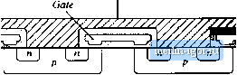 Minority carrier injection t t Collector FiK. 4.38 rlie IGBT: (a) bchematic symbol, (b) equivalent eircuit. Gate Emitter The funetion of the added p region is to injeet minority charges into the ;( region while the device operates in the on state, as illu.strated in Fig. 4.37. When the IGBT conducts, the p-n junction is forward-biased, and the minority charges injected into the ft region cause conductivity modulation. This reduces the on-resistance of the n~ region, and allows high-voltage IGBTs to be constructed which have low forward voltage drops. As of 1999, IGBTs rated as low as Ш) V and as high as 33(Xi V are readily available. The forward voltage drops of these devices are typically 2 to 4 V, much lower than would be obtained in equivalent MOSFETs of the same silicon area. Several schematic symbols for the IGBT are in current use; the symbol illustrated in Fig. 4.38(a) is the most popular. A two-transistor equivalent circuit for the IGBT is illustrated in Fig. 4.38(b). The IGBT functions effectively as an u-channel power MOSFET, cascaded by a PNP emitter-follower BJT. The physical locations of the two effective devices are illustrated in Fig. 4.39. It can be seen that there are two effective currents: the effective MOSFET channel current and the effective PNP collector current ij. The price paid for the reduced voltage drop of the IGBT is its increased switching times, especially during the turn-off transition. In particular, the IGBT turn-off transition exhibits a phenomenon known as current tailing. The effective MOSFET can be turned off quickly, by removing the gate charge such that the gate-to-emitter voltage is negative. This causes the channel current ( j to quickly become zero. However, the PNP collector current continues to flow as long as minority charge is present in the ff region. Since there is no way to actively remove the stored minority charge, it slowly decays via recombination. So /2 slowly decays in proportion to the minority charge, and a current tail is obsened. The length of the current tail can be reduced by introduction of recombination centers in the ~ region, at Emitter 2ZZ ZD Fig. 4.39 Physical locutions of the effective MOSFET and PNP components of the latiT. TZZZ ..J. /J / о Collector |