
|
| |
Строительный блокнот Introduction to electronics 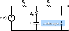 4 < Fig, C.IO R-C circuit example of Section C.4.i, wliere Z(j) is llie capacitor inapedance lIsC. The impedance Zj,(j) is the Thevenin eqiiivalenl impedance seen at the port where the capacitor is cotitiected. As illtistrated in Fig. C. 12(a), this impedance i.s foutid by setting the indepetident souice to zero, and then determining the impedance between the port termitials. The result is: (C.31) Figure C.12(b) illustrates determination ofthe impedance Zj). A current source \(s) is connected to the port, in place of the capacitor. In the presence ofthe input v{s\ the current source r(.?) is adjusted so that the output Vj(s) is nulled. Under these null conditions, the impedance Zj) is found as the ratio of v{s) to \{s). Il is easiest to find Z(i) by first determining the elTecl ofthe null condition on the signals in the circuit. Since is nulled to zero, there is no ctirrent through the resistor Д4. Since is connected in series with Я, there is also no cunent through Д and hence no voltage across R.. Therefore, the voltage V, in Fig. C. 12(b) i.s equal to v, i.e.. j null Therefore, the voltage v is given by /Д;. The impedance Z is (C.32) Fig. C.ll Manipulation of the circuit v{s) Ci ai Fig. C, 10 into the form of Fig. C. I. 1 -ЛЛг Linear circuit ЛЛ/- port ЛЛг- port t ЛЛ/-T-\f\r- port 4 S V,(S) null Fig, C,I2 MeasLueiTient of the quantitLes Z(,!) and Z,)(j): (aJ deter-ininaiioii of Z,j(.v), (b) tleterniination <>f7 (.v) (CB) Note that, in general, the independent sources and ( are nonzero dtiring the measurement. For this example, the null condition implies that the current i(s) flows entirely through the path composed of K, R, and V. The transfer function G(s) is found by substitution of Eqs. (C.31) and (C.33) into Eq. (С.ЗО): c(.0 = a 1 + .vC r2 + Wll(f, + (CM) For this example, the result is obtained in standard normalized pole-zero form, because the capacitor is the only dynamic element in the circuit, and because the original conditions, in which the capacitor impedance tends to an open circuit, coincide with dc conditions in the circuit. A similar procedure can be applied to write Ihe transfer function of a circuii, containing an arbitrary number of reactive elements, in normalized form via an extension of the Extra Elemeni Theorem [3], C.4.2 An Unmudeled Element We are told that the transformer-isolated parallel resonant inverter of Fig. C.13 has been designed with the assutnption that the transformer is ideal. The approxitnate sinusoidal analysis techniques of Chapter 19 were employed to inodel the inverter. It is now desired to specify a transformer; this requires that limits be specified on the minimum allowable transformer magnetizing inductance. One way to approach this problem is to view the transformer magnetizing inductance as an extra element, and to derive conditions that guarantee that the presence ofthe transformermagnetizing inductance does not significantly change the tanlc network transfer function G(s). Figure C.14 illustrates the equivalent circuit model of the inverter, derived using the approximate sintisoidal analysis technique of Section 19.1. The switch network output voltage vДt) is modeled by its fundamental component vil), a sintisoid. The tank transfer function Gis) is given hy: vjs) (C,35) 1 :я Fig. C,I3 Parallel resonant inverter example. Transfer function 1 : n Fig. C.14 Equivalent circuit model ofthe tank network, based on the approximate sinusoidal analysis technique. |