
|
| |
Строительный блокнот Introduction to electronics 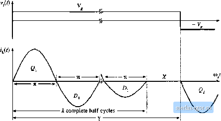 Fig, 19.43 Tank inductor uuirent waveform, type it DCM, for tven A. Fig, 19,44 Steady-state equivalent circuit model for ati even discontinuous conduction mode: an effective gyratoi-. The tjnuverter exhibits current source characteristics.  Tlie tesLiit is shown in Fig. 19.45, and tlie mode boundaries are explicitly diagrammed in Fig. 19.46. It can Ъе seen that, for operation above resonance, the only possible operating mode is the к = 0 CCM, and that the output voltage decreases monotonicaiiy with increasing switching frequency. Reduction in ioiid curretit (t)r incieiLse in load resistance, which decreases Q) causes the output voltage to increase. A number of successful designs that operate aixive resonance and utilize zero-voitage switching have been documented in the literature [7,21]. Operation below resonance is complicated by the presence of subhartnonic and discontinuous conduction tnodes. The к = 1 CCM and i = 2 DCM are well behaved, in that the output voltage increases monotonically with increasing switching frequency. Increase ofthe load current again causes the output voltage to decrease. Successful designs that operate in these mtxies and employ zero-current switching are numerous. However, operation in the higher-order tnodes {k = 2 CCM, t = 4 DCM, etc.) is normally avoided. Given F and Q, the operating mode can be evahiated directly, using the following algorithm. First, the continuou.s conduction mode к corresponding to operation at frequency f with heavy loading is found: *=int(1) where lNT(jc) denotes the integer part of л. Next, the quantity fc, is determined: (19.90) 1-it 0.9 0.8 0.7 0.6 0.5 0.4 0.3 0.2 O.l 0
2 = 0.2 0,35 0.s 0,75 1 1.3 2 C=zo 0.8 1 i.2 Fig. 19.45 Complete eonlroi plane thaiaeteiistics of the series resonant converter, for the range 0.2 <, /£2. к=IDCM 0.9 0,8 0,7 0.6 0,5 0.4 0.3 0.2 0.1 0 Jt = 3 DCM . ;k i\ Cpk : j Jt = 4 , DCM etc. *\ . jtKOCCM-., Fig. 19.46 Contihuous anJ discontinuous conduction mode boundaries. 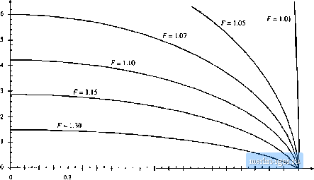 0.4 0,6 Fig. 19.47 Output cltaructeristics, J: = 0 CCM (above resoriance). t,=INT The conveiter operates in type к CCM providetJ that: (19.91) (19,92) Otherwise, the converter operates in type DCM. A simple algorithm can therefore be defined, in which the conversion ratio M is computed for a given F and Q. First, Eqs, (19.90) to (19,92) are evaluated, to determine the operating mode. Then, the appropriate equation (19.83), (19.85), or (19.88) is evaluated to find M. Giitpiit l-V plane characteristics for the к = 0 CCM, plotted using Eq. (19.79), are shown in Fig. 19.47. The constant-frequency curves are elliptical, and all pass through the point M = I, У = 0. For a given switching frequency, the operating point is given by the intersection ofthe elliptical converter output characteristic with the load /-V characteristic. Output plane chiu-acteristics that combine the к = 1 CCM, к = 1 DCM, and к = 2 DCM are shown in Fig. 19.48. These were plotted using Eqs. (19.79), (19.85), and (19.ss). These curves were plotted with the assumption that the transistors are allowed to conduct no longer than one tank half-cycle during each switching half-period; this eliminates siibharmonic modes and causes the converter to operate in t = 2 ori = 1 DCM whenever/j < 0.5/(,. Jt can be seen that the constant-frequency curves are elliptical in the continuous conduction mode, vertical (voltage source characteristic) in the t = 1 DCM, and horizontal (current source characteristic) in the = 2 DCM. |
|||||||||||||||||||||||||||||||||||||||||||||||||||||||||||||||||||||||||||||||||||||||||||||||||||||||||||||||||