
|
| |
|
Строительный блокнот Introduction to electronics Fig. 19.27 Switch network output: waveforms for the series lesonaiit convener, operated above resonance in the continuous conduction mode. Zero-voltage switching aids the transistor turn-on process. 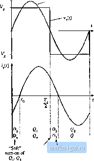 Conducting dtvices: ~/ Hard Soft Hard tum4>(Tof turaon of nim-offof transistor on. With a minor circuit modification, the transistor turn-off transitions can also be caused to occur at zero voitage, Tliis process can iead to significant reductions in the switching losses of converters based on MOSFETs and diodes. For the full bridge circuit of Fig. 19,24, the switch output voltage Vj(f), щк! its fundamental component fj](0. as well as the approximately sinusoidal tank cnrrent waveform ij.t), ate plotted in Fig. 19.27. At frequencies gteater than the tank resonant frequency, the input impedance of the tank network Z((j) is dominated by the tank inductor impedance. Hence, the tank presents an effective inductive load to the bridge, and the switch current /) lags the switch voltage fundamental component as shown in Fig. 19.27. In consequence, the zero crossing of the voltage waveform vp) occurs before the current waveform iJJ). Forthe half cycle 0<f< 7/2, the switch voltage vt) is equal to-l- V. F()rO</< the current /j(j) is negative and diodes D and conduct. Tiansi.stois Q and conduct when ijj.) \s, positive, over the interval t<l< Tjl. The waveforms during TJ2 <I<T are symmetrical. Since the zero crossing of v,(t) leads the zero crossing ofr/t). the transistors conduct after their respective antiparallel diodes. Note that, at any given time during the Dj conduction interval 0< t < t, transistor Q, can be turned on without incurring switching loss. The circuit naturally causes the tratisistor turn-on tiansition tt) be lossless, and long turn-on switching titnes can be tolerated. A particularly significant implication of this is that the switching loss associated with reverse recovery of the antiparallel diodes is avoided. Relatively slow diodes, such as the MOSFET body diodes, can be einployed ftw realization of diodes D, to Л, In addition, the output capacitances of transistors Q, to and diodes D, to do not lead to switching loss. In general, zeio-vt)ltage switching can occur when the resonant tank presents an effective inductive load to the switches, atid hence the switch vohage zero crossings occur before the switch current zero crossings. In the bridge configuration, zero-voltage switching is characterized by the half-bridge conduction sequence D-Qi-DQi such that the transistors are turned on while their respective antipar- 19.3 S/>fi Switching Fig. 19.28 TVansistor voltage and current waveforms, for Operation of the series resonant converter above resonance in the it = 0 CCM. Conducting devices: 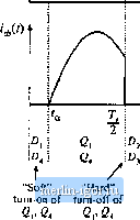 allel diodes conduct. Since the transistor voltage is zero during the entire turn on transition, switching loss due to slow turn-on titnes or due to energy storage in any ofthe device capacitances does not occur at turn-on. The transistor turn-off transition in Fig. 19.28 is simihu to that of a PWIVI switch. In converters that employ IGBTs or other minority-carrier devices, significant switching loss may occur at the turn-off transitions. The curtent tailing phenotnenon causes 2t pass through a period of high instantaneous power dissipation, and switching loss occurs. To assist the transistor turn off process, small capacitors Cj, may ije intrrxluced into the legs of the biidge, as detnonstrated in Fig. 19.29. In a converter etnpioying MOSFETs, the device output capacitances iire sufficient for this puipose, with no need forcAtemai discrete capacitors. A delay is iiiso introduced into the giite drive signals, so that there is a shott commutation interval when all four transistors are off. During the normal Qj, D, Qj, iind D- conduction intervals, the leg capacitors appear in parallel with the semiconductor switches, iind have nu effect un the conveiter operation. However, these capacitors introduce commutation intervals at transistor turn-off. When C[ is turned off, the tiinlc current 1ДГ/2) flows through the switch capacitances Cy instead of G[. and the voitiige across and C,j increases. Eventually, the voitiige iicross й reaches V; ditxle then ijecotnes forward-biased. If the MOSFET turn-off titne is sufficiently fast, then the MOSFET is switched fully off before the drain voltage rises significantly above zero, and negligible turn-off switching loss is incurred. The energy stored in the device capiicitances, that is, in С,, is transferred to the tanlt inductor. The fiict that none of the .semiconductor device capiicitances or stored charges lead to switching loss is the miijor advantiige of zero-voitiige switching, and is the most common niotivation for its use. MOSFET converters can typically be operiited in this inanner, using only the internal draiti-to-source capacitances. However, other devices such as IGBTs typically require substantial external capacitances to reduce the losses incurred during the IGBT turn-off transitions. An additional advantage of zero-voltage switching is the reduction of EMI iLssociated with device capacitances. In conventional PWM converters and also, to some extent, in zero-current switching converters, significant high-frequency ringing iind curretit spikes are generated by the rapid chiugitig and discharging ofthe semiconductor device ciipacitances during the turn-on and/or turn-off transitions. v,(0 (o remainder of converter Fig. 19.29 IntroductiDfi of small capacitors Cj, which reduce the tum-off-lransition switching loss when the series resonant converter is operated above resonance: (a) bridge circuit, (b) iransistor voltage waveform. Condiiciing devices: Turn off / Commutation interval Ringing is conspiciiotisly absent from the waveforms of converters in which all semiconductor devices switch at zero voltage; these converters inherently do not generate this type of EMI. 19.4 LOAD-DEPENDENT PROPERTIES OF RESONANT CONVERTERS The properties of the CCM PWM converters studied in previous chapters are largely unaffected by the load cnrrent. In consequence, these converters exhibit several desirable properties that are often taken for granted. The transistorcurrent is proportional to the load current; hence conduction losses become small at light load, leading to good light-load efficiency. Also, the otitput impedance is low, and hence the dc output voltage does not significantly depend on the load t-v characteristic (at least, in CCM), Unfortunately, these good properties are not necessarily shared by resonant converters. Of central importance in design of a resonant converter is the selection of the resonant tank topology and element values, so that the transistor conduction losses at light load are rainimized, so that zero-voltage switching is obtained over a wide range of load currents (preferably, for all anticipated loads, but at least at full and intermediate load powers), and so that the converter dynamic range is compatible with the load !-v characteristic. These design issues are addressed in this section. The conduction loss caused by circulating tank currents is well-recognized as a problem in resonant converter design. These ctirrents are independent of, or only weakly dependent on, the load current, and lead to pt)or efficiency at light load. In Fig. 19.30, the switch current is) is equal to v,(j)/Z;(i). If we want the switch current to track the load current, then at the switching frequency Z; should be dominated by, or at least strongly influenced by, the load resistance R. Unfortunately, this is often not consistent with the requirement for zero-voltage switching, in which is dominated by a tank inductor. |