
|
| |
|
Строительный блокнот Introduction to electronics In a fixed-frequency systera, T, is constant, and tlie integral over one switching periotJ is proportional to the average valtie. Hence the average switch ctirrent can be controlled to be proportional to a refetnce signal by sintply switching the transistor off when tlie integral of tlie switch ctirrent is eqtial to the reference. In the controller of Fig. 18.21. tlie switcli ctirrent i/f)is scaled by the transfortnerturns ration, and tlien integrated by capacitor C-, such that v,W = The integratorvoltage v,(.f) is reset to zero at the etid of each switchitig period, and the integration process begins anew at the beginning of the next switcliing period. So at the instant lhat Ihe transistor is switched off, the voltage vfdJ) is proportional to the average switch current: Vi№ = for interval 0<f<r, How should the average switch current be controlled? To obtain input resistor emulation, it is desired thai . , Мз, (1 .74) It is further desired to avoid sensing either i(f) or v{t). As with other schemes, we will sense the dc output voltage {vit)\, to construct a low-bandwidth feedbaclc loop that balances the average inptit and output powers. So let us determine the relationship between and {vit)\ implied by Eq. (18.74). If we assume that the boost conveiter operates in the continuous conduction mode, then we can write (j,(f))., = rf(()(,(0) <18.75) {v,il))=d[t){v(t)) (18.76) Substitution of Eqs. (18.75) and (18.76) into Eq. (18.74) leads to ¥)t. (18.77) (fir)),=*)(l-r/(0) The controller of Fig. 18.21 implements this equation. The nonlinear carrier generator of Fig. 18.21 produces the parabolic wavefortn vjj), given by for a<t<T, (18,78) This waveform is illustrated in Fig. 18.22. Note lhal Eq. il8.7K) resembles Eq. (18.77), with d(t} replaced by (l/T), The controller switches the transistor off at lime ( = dT when the integrator vohage fj(r) is equal lo the carrier waveform v/t). Hence, it is true lhal vdT,) = v,(dT,) = v , r) dU) {1 - d(.t)] Substitution of Eq. (18.73) yields {iM)-,. - = v, JJ)dit){l-d(jy] (18,79) (18.80) This is of the same form as Eq. (18.77). Comparison of Eqs. (18.77) and (18.80) reveals that the emulated resistance is given by (18.81) Ifthedc output voltage and the control vollage have negligible ac variation, then R is essentially constant, and the ac line current will exhibit low harmonic distortion. So neither the input voltage nor the input current need be sensed, and input resistor emulation can be obtained in CCM boost converters by sensing only die swilch current. A simple way lo generate the parabolic carrier waveltirm uses two integrators, as illustrated in Fig. 18.23. The slowly varying control voltage Vjo ,j{f) is integrated, to obtain a ramp waveform v,(0 whose peak amplitude is proportional to f j,j, ,(f). The dc component of this waveform is removed, and then integrated again. The ouipul of lhe second integrator is the parabolic carrier v.(l), illij.strated in Fig. 18.22 and given by Eq. (1K.7S), Both integrators are reset to zero before the end of each switching period Removal of dc ......., component Integrator with reset iClock Fig. 18.23 CkTieration of parabolic carrier waveform by double integration. 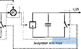 1S.4 Siiigk-Fluise Converter Sysrems Incorporating Ideal Rectifiers 663 by the dock generator. The amplitude of the parabolic canier, and hence also the emulated resistance, can be controlled by variation of i( t fM. Equations (18.75) atid (18.76) are valid only when the converter operates in the eotitintious coti-ductioti mode. In consequence, the ac line ctirrent waveform is distorted when the converter operates in DCM. Since this occurs near the zero crossings of the ac line voltage, crossover distortion is generated. Nonetheless, the harmonic distortion is less severe than in current-programmed schemes, and it is feasible to construct universal-input rectifiers that employ the NLC control approach. Total harmonic distortion is analyzed and plotted in [28]. Nonlinear carrier control can be applied to current-programmed boost rectifiers, as well as to other rectifiers based on the buck-boost, SEPIC, Cuk, or other topologies, with either integral charge control or peak-current-programmed control [28,29]. In these cases, a different carrier waveform must be employed. A nonlinear-carrier controller in which the ac input vohage v{t) is sensed, rather than the switch current i (f), is described in [30]. 18.4 SINGLE-PHASE CONVERTER SYSTEMS INCORPORATING ШЕАЬ RECTIFIERS An additional issue that arises in PWM rectifier systems is the control of power drawn from the ac line, the power delivered to the dc load, and the energy stored in a bulk energy storage capacitor. 18.4.1 Energy Storage It is usually desired that the dc output voltage of a converter system be regulated with high accuracy. In practice, this is easily accomplished using a high-gain wide-bandwidth feedback loop. A well-regulated dc output voltage v(i) = V is then obtained, which has negligible ac variations. For a given constant load characteristic, the load current / and the instantaneous load power Pi i,A) = also constant: /WO = v(/)/{r)= W (1я.82) However, the instantaneous input power p.{i) of a single-phase ideal rectifier is not constant: If v ) is given by Eq. (18.11). and if i/O follows Eq. (18.1), then the instantaneous input power becomes PJO = sin (tut) = (] - eo.s (2tat)) ( which varies with time. The instantaneous input power is zero at the zero crossings of the ac input voltage. Equations (18.82) and (18.84) are illustrated in Fig. 18.24(a). Note that the desired instantaneous load power PijO) is not equal to the desired instantaneous rectifier input power p i()- Some eieiiient within the rectifier system must supply or consume the difference between these two instantaneous powers. Since the ideal rectifier does not consume or generate power, nor does it contain significant internal energy storage, it is necessary to add to the system a low-frequency energy storage eletneiit such |