
|
| |
|
Строительный блокнот Introduction to electronics corresponding to this equation is then constructed. In the case of the buck converter, as well as in other converters having pulsating input ciirrent.4, this equivalent circuit contains a dependent current source which becomes the primary of a dc transformer mtidel. In the bot)St converter example of Section 3.3, it wa.4 unnecessary to explicitly write this equation, Ьесаи.че the input current (,(0 coincided with the inductor current i(t), and hence a complete equivalent circuit could be derived using only the inductor voltage and capacitor current equations. 3.5 EXAMPLE: INCLUSION OF SEMICONDUCTOR CONDUCTION LOSSES IN THE BOOST CONVERTER MODEL As a final example, let us consider modeling .semiconductor conduction lo,4se,4 in the boo.st converter of Fig. 3.22. An[)ther major source of power loss is the conduction loss due to semiconductor device forward voltage drops. The forward voltage of a metal oxide semiconductor field-effect transi.stor (MOSFET) or bipolar junction transistor (BIT) can be modeled with reasonable accuracy as an on-resistance fi . In the са.че of a diode, in.sulated-gate bipolar transistor (IGBT), or thyri.stor, a voltage .source plus an on-resistance yield.s a model of g(K)d accuracy; the on-resistance may be omitted if the converter is being modeled at a .single operating point. When the gate drive signal is high, the MOSFET turns on and the diode is reverse-biased. The circuit then reduces to Fig. 3.23(a). In the conducting state, the MOSFET is modeled by the on-resistance The inductor winding resistance is again represented as in Fig. 3.5. The inductor voltage and capacitor current are given by v,il)-V-iK,-iK V-/ii,-/R, (3.27) The inductor current and capacitor voltage have again been approximated by their dc components. When the gate drive signal is low, the MOSFET turns off The diode becomes forward-biased by the inductor current, and the circuit reduces to Fig. 3.23(b). In the conducting state, the diode is modeled in this example by voltage source V and resistance liy The inductor winding resistance is again modeled by resistance /(,.The inductor voltage and capacitor current for this subinterval are yU) = - iR, - V - ,R - V = V, - lit, - V -IR -V i.(0=<- = /- The inductor voltage and capacitor current waveforms are sketched in Fig. 3.24. (3.2Я) ТППГ Fig, 3,12 Boost cooveiter example. 3.5 Kmmple: liidmim of Semiconducior Conduction Losses in the ВмкЯ Convener Model S3 тггпг ЛЛ-I + V, - -TIPS + V, ---W- Fig. 3.23 Boost converter drcuits: (a) when MOSFET conducts, (b) when diode conducts. The dc component of the inductor voltage is given by By collecting terras and noting that D + D - i., one obtains V -IRr- IDR, - DV - IDRi, - DV = 0 (3.29) (3,30) This equation describes the dc components of the voltages around a loop containing the inductor, with loop current equal to the dc inductor cuuent /. An equivalent circuit is given in Fig. 3,25, Fig, 3.24 Indactor voliage vlf) and capacitor current i(t) wavefoinis, for the converter of Fig. 3.22,
Mg. 3.25 Equivalent circuit currespunding \o tiq, (3.30). ЛЛг Hg, 3.36 Equivalent circuit corresponding to Eq. (3,32). 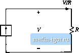 Thie dc component of the capacitor current is (/,) = D(-)tf(/-) = 0 Upon collecting terms, one obtains (3.31) (3.32) This equation describes the dc components of the currents flowing into л node connected to the capacitor, with dc capacitor voltage equal to V. Ati equivalent circuit is given in Fig. 3.26. The two circuits are drawn together in 3.27. The dependent sources are combined into an ideal 1У: 1 transformer in Fig. 3.28, yielding the complete dc equivalent circuit model. Solution of Fig. 3.2S for the output voltage V yields (3.33) © DR.... Z Offn АЛ- ЛЛг- 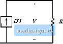 Fig. 3.27 The circuits of Figs, 3,25 and 3.26, drawn together |
|||||||||||||||||||