
|
| |
|
Строительный блокнот Introduction to electronics Table 1(1.1 Input (ilter design criteria for basic converters Converter ZtJs) Zois) Buck Bi30st Buck-boost iV2j 1 +J [l + sRC] 1 +j: {l+sRC) wliere (10.S) is tlie original control-to-output transfer function witli no input filter. Tliequantity Zp(s) is equal to tlie converter input impedance Z.(s) under the condition thatf/(j) is equal to zero: (10.6) The quantity Z,(i) is equal to the converter input impedance Z.v) under the condition that the feedback controller of Fig. 10.5 operates ideally; in other words, the controller varies as necessary to maintain v(x) equal to zero: 2 (*)-адЦ, (10-7) In terms of the canonical circuit model parameters described in Section 7.5, Z(.v) can be shown to be Expressions for Zji) and 2(5) for the basic buck, boost, and buck-boost converters are listed in Table 10.1. 10.2.1 Diu&siun Equation (10.4) relates the power stage control-to-output transferfunction С.Дг) to the output impedance ZJa) of the input filter, and also to the quantities Zis) and ZJis) measured at the power input port of the converter. The quantity ZC?) coincides with the open-loop input impedance of the converter. As described above, the quantity Zj) is equal to the input port impedance of the converter Closed-loop {\ {tfj ,...}!?.l(§.?..f.S. ..!..?.L.., .........j 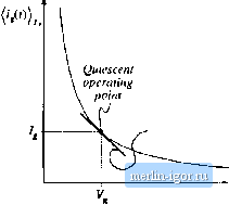 Fig, 10,7 Power input part cltiiracieristics of nn idenl switthing voltage regulator: (a) equivalent circuit itioUd, including dependent power sink, (b) constant power characteji&tic of inpjit port. power stage, under tlie conditions tliat dis) is varied as necessary to null v{s) to zero. This is, in fact, the function performed by an ideal controller: it varies the duty cycle as necessary to maintain zero error of the output voltage. Therefore, ZfJs) coincides with the impedance that would be measured at the converter power input terminals, if an ideal feedback loop perfectly regulated the converteroutput voltage. (3f counie, Eq. (10.4) is valid in general, regaidless of whether a control system is present. Figure 10.7 illustrates the large-signal behavior of a feedback loop that perfectly regulates the converter output voltage. Regardless of the applied input voltage v.(/), the output voltage is maintained equal to the desired value V. The load power is therefore constant, and equal to P = V/R. In the idealized case of a lossless converter, the power flowing into the converter input terminals will also be equal to Pi, i, regardless of the value of v)- Hence, the power input terminal ofthe converter obeys the equation (10.9) This characteristic is illustrated in Fig. 10.7(b), and is represented in Fig. 10.7(a) by the dependent power sink symbol. The properties of power sources and power sinks are discussed in detail in Chapter 11. Figure l().7(b) also illustrates linearization of the constant input power characteristic, about a quiescent operating point. The resulting line has negative slope; therefore, the incremental (small signal) input resistance ofthe ideal voltage regulator is negative. For exatnple, ittcreasing the voltage (v(t))j. causes the current (г (/)to decrease, such that the power remains constant. This incremental resistance has the value [9,14]: --Д. (10,10) where R is the output load resistance, and M is the conversion ratio V/V. For each of the converters listed in Table 10.1, the dc asymptote of Z,j(j-) coincides with the negative incremental resistance given by the equation above. EVactical control systems exhibit a limited bandwidth, determined by the crossover frequency of the feedback loop. Therefore, we would expect the closed-loop regulator input impedance to be approxiinately equal to Zjy(j) at low frequency (f /.) where the loop gain is large and the regulator works well. At frequencies above the bandwidth of the regulator (f3> /j), we expect the converter input impedance to follow the open-loop value ZqU). For closed-loop conditions, it can be shown that the regulator input impedance Z/(,s) is, in fact, described by the following equation: 1 , (10,11) 4s) Zis) 1 + ns) Z (s) I + T{s) where J\s) is the controller loop gain. Thus, the regulator input impedance follows the negative resistance of Z(.i) at low frequency where the magnitude of the loop gain is large [and hence Г/(1 +T) = 1, 1/(1 + I) = 0], and reverts to the (positive) open-loop impedance Zp(s) at high frequency where 7 is small [i.e., where T/(l -I-Г) = {), 1/(1 +7)= 1]. When an undamped or lightly damped input filter is connected to the regulator input port, the input filter can interact with the negative resistance characteristic of to form a negative resistance oscillator. This further explains why addition of an input filter tends to lead to instabilities. 10.2.2 Impedance Inequalities Equation (10.4) reveals that addition of the input filter causes the control-to-output transfer function to be modified by the factor (10.12) called the correction factor. When the following inequalities are satisfied, and jjj Z.-i2o[ then the correction factor has a magnitude of approximately unity, and the input filter does not substantially alter the control-to-output transfer function [9,10]. These inequalities limit the maximum allowable output impedance of the input filter, and constitute useful filter design criterta. One can sketch the Bode plots of 11 II and SI Z[,0(U) II, and compare with the Bode plot of II ZJjVi) . This allows the engineer to gain the insight necessary to design an input filter that satisfies Eq. (10.13). |